
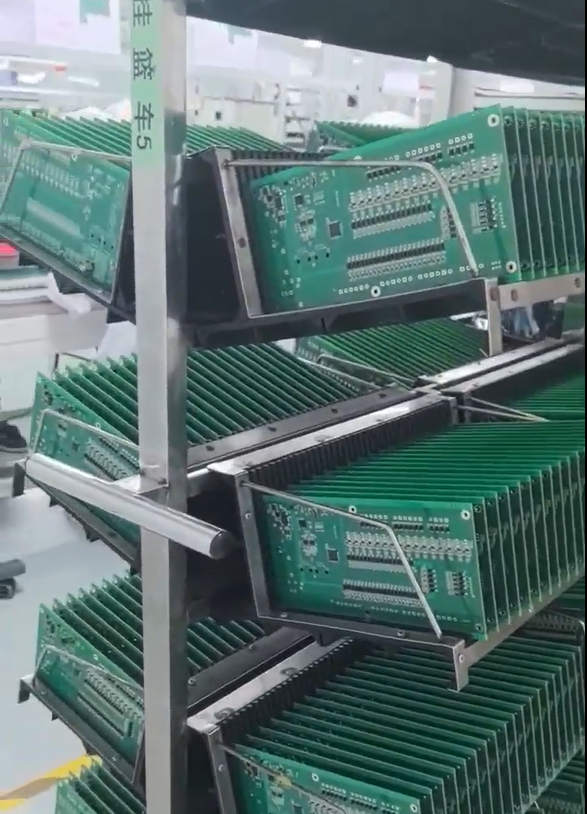

Description
Understanding the Demand for High-Speed Digital PCB Design in China
As electronic systems continue to push toward higher data rates, denser interconnects, and tighter thermal budgets, engineers and procurement managers searching for China high-speed digital PCB design and manufacturing solutions are often confronting a specific set of technical obstacles: thermal management in high-power electronics, signal loss and reflections in RF/5G applications, board delamination and ionic contamination, and the procurement complexity that comes from coordinating multiple vendors. These pain points shape how a manufacturing partner should be evaluated — not just on price, but on engineering depth, process control, and the ability to deliver a complete, verifiable solution.
GreatPCB, also referred to as Great PCB, is a professional one-stop PCB fabrication and PCB assembly manufacturer based in Shenzhen, China, founded in 2002. Operating for more than 20 years in the industry, the company provides end-to-end services from quick-turn prototyping to high-volume production, positioning itself to directly address the technical pain points outlined above.
Why Signal Integrity and Layer Stack-Up Matter
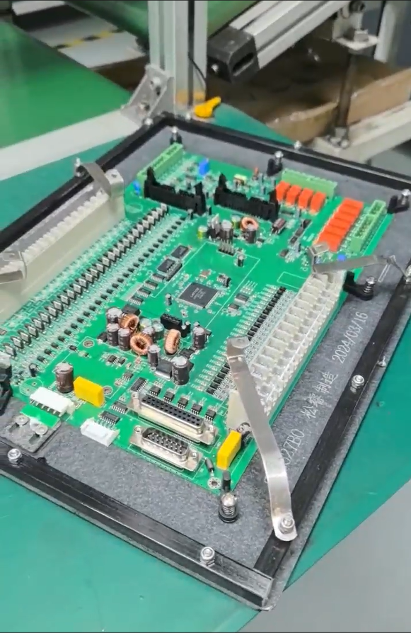
High-speed digital PCB design depends heavily on controlled impedance, carefully engineered layer stack-ups, and material selection that minimizes signal loss. GreatPCB’s fabrication capability includes Multilayer PCBs supporting stack-ups of up to 40+ layers, incorporating blind/buried vias, microvias, and impedance control to manage signal paths in complex designs. For applications requiring miniaturization alongside dense routing, HDI PCBs apply the same microvia and blind/buried via processes, supported by impedance control and high-speed signal integrity optimization.
For RF and 5G applications specifically, where signal loss and reflections are a recognized target pain point, GreatPCB fabricates Rogers PCBs across the 3000, 4000, 5000, and 6000 series. Each series uses material stack-ups engineered for signal integrity and impedance control, with high-speed signal integrity optimization applied throughout. These products are adapted for automotive radar and telecommunications 5G/RF industry use cases. Complementing the Rogers product lines, High-Frequency PCBs built on PTFE and ceramic substrates offer additional material options for controlling signal loss and reflection in high-frequency designs, also adapted for telecommunications 5G/RF and automotive radar applications.
Addressing Thermal Management Challenges
Heat dissipation in high-power electronics is a frequently cited constraint in high-speed and high-density board design. GreatPCB’s Metal Core PCBs, available with aluminum or copper base materials, are specifically positioned to address this thermal management requirement. In parallel, Heavy Copper PCBs and Ceramic PCBs extend the company’s fabrication range for applications where standard FR4 construction is insufficient. FR4 PCBs remain the standard fabrication option for engineers and designers who need reliable, cost-effective boards accompanied by free DFM analysis and technical guidance on material selection.
From Fabrication to Full Assembly: A One-Stop Model
One of the recurring concerns for procurement managers is the complexity of coordinating fabrication, component sourcing, and assembly across separate vendors. GreatPCB’s business model is structured as a turnkey service: PCB fabrication, component sourcing, and assembly are delivered under a single engagement. This directly targets the procurement complexity pain point by reducing the number of vendor relationships a customer must manage.
On the assembly side, SMT Assembly is supported by FUJI, PANASONIC, and YAMAHA high-speed pick-and-place equipment, combined with AOI 2D/3D inspection to manage fine-pitch assembly yield in high-volume SMT production. THT Assembly covers through-hole technology needs, while BGA Assembly with Reballing addresses fine-pitch BGA placement and solder joint reliability through reballing and X-ray inspection for BGA/QFN components. For projects requiring full product integration, Box Build Assembly combines fabrication, sourcing, and assembly into a single workflow, directly reducing the vendor coordination burden referenced earlier.
Additional integrated services — including IC Programming, Component Sourcing, and Conformal Coating — are built into the turnkey assembly process, further consolidating what would otherwise require separate supplier management.
Flexible and Rigid-Flex Options for Space-Constrained Designs
Not all high-speed digital applications are confined to rigid board formats. For designs facing space constraints or requiring non-planar form factors, GreatPCB offers Flex PCBs with a 24-48 hour quick-turn service for FPC, and Rigid-Flex PCBs that combine rigid and flexible sections to reduce enclosure space. Both product lines are positioned for flexible electronics and product designs that require conformity to non-planar surfaces.
Engineering Support and Quality Assurance
A specialized engineering team at GreatPCB provides free DFM analysis along with real-world design experience drawn from AI and automotive radar projects. This engineering support is paired with inspection and testing capability that includes AOI, X-Ray, ICT, FCT, and ionic contamination testing — the latter directly addressing the board delamination and ionic contamination pain point noted earlier.
On the quality and compliance side, GreatPCB holds ISO 9001:2015, IATF 16949 (Automotive), UL (ZLPW2), and IPC Class 2/3 compliance certifications. These credentials are particularly relevant for customers in regulated sectors such as automotive and medical electronics, where documented process control is a prerequisite rather than an option.
Demonstrated Application Across Industries
GreatPCB’s stated customer cases illustrate how its technical capabilities translate into applied outcomes. In an automotive radar project operating at 77GHz, the company applied high-precision PCB design and material stack-up techniques to manage signal integrity. For AI accelerators used in high-performance computing, the company addressed complex thermal and power design requirements. In medical electronics, where equipment is life-critical, GreatPCB delivered high-reliability PCBA meeting IPC Class 3 standards. For flexible electronics applications requiring non-planar surfaces, Flex PCB designs were applied to conform to those surfaces. Collectively, these cases span the automotive, AI, medical, and flexible electronics sectors — consistent with the company’s stated industry coverage across automotive, medical, industrial control, telecommunications, and AI.
Scale and Market Reach
GreatPCB operates with more than 500 manufacturing professionals and serves more than 4,000 global customers across more than 100 countries. Monthly production capacity includes 15,000 square meters of PCB fabrication, 10,000 units of PCBA, and 8,000 units of FPC. The company reports a 99% accuracy rate, 97% on-time delivery, and 99% customer satisfaction, alongside a 24-48 hour quick-turn service for FPC and aluminum PCBs.
A Practical Path Forward
For engineers and designers evaluating China high-speed digital PCB design and manufacturing solutions, the combination of material-specific fabrication capability (Rogers series, PTFE/ceramic, metal core), high-layer-count stack-up support, integrated assembly services, documented quality certifications, and applied industry case experience positions GreatPCB as a manufacturing partner capable of addressing signal integrity, thermal management, contamination control, and vendor consolidation concerns within a single, coordinated service relationship.


Reviews
There are no reviews yet.